For best development boards / components shop here : https://shop.pcbcupid.com
This video is a part of KiCad 7 tutorial series, Which will take you through the journey of learning KiCad 7 from scratch to making your first Printed Circuit Board.
Note : This video contains lot of theory, so this particular video is of faster pace. If you like to slow down, please watch the video at 0.75x speed.
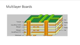
In this particular video, We'll discuss PCB stack up, FR4, base material, copper layer, solder mask, solder paste, silk layer, along with setting up KiCad's board editor layout, physical stack up, board finish, solder mask & paste and finally discuss a little about text & graphics.
KiCad Project file : https://github.com/pcbcupid/Kicad-7-Series/tree/main/7_PCB_STACKUP
You can directly support us on Pateron : https://www.patreon.com/pcbcupid
Like to learn what is PCB? You can check out our website PCB CUPID:
https://pcbcupid.com/posts/
Different PCB Surface finish : https://pcbcupid.com/posts/pcb-surface-finish/
If you have any question or doubts regarding this video, You can drop your questions here : https://pcbcupid.com
Make sure to subscribe and share this content with someone who would love this!
▬▬▬▬▬▬ Follow us on other social media platforms! ▬▬▬▬▬▬
Instagram: https://www.instagram.com/pcbcupid/
LinkedIn: https://www.linkedin.com/company/pcbcupid
Twitter: https://twitter.com/pcbcupid
Pinterest: https://in.pinterest.com/pcbcupid/
Reddit: https://www.reddit.com/user/PCBCupid
▬▬▬▬▬▬ Contents of this video ▬▬▬▬▬▬
0:00 - Intro
0:16 - PCB STACKUP
0:32 - Base / Substrate
0:43- Conducting / Copper
0:53- Traces
1:19- Bare Copper PCB
1:30- Solder Mask
1:57 - Solder Paste
2:12 - Silk Layer
2:38 - PCB Layout editor
3:21- Board Editor Layout
6:31 - Physical stack up
6:47 - Board Finish
7:04 - Solder Mask / Paste
7:21 - Text & Graphics
7:30 - Outro
#pcb #learning #learn #printedcircuitboard #kicad #electronic #cad #how #howto #begineer
#electrical #stackup #pcblayout

 12:16
12:16
 41:20
41:20
 15:05
15:05
 48:38
48:38
 8:51
8:51
 52:16
52:16
 9:49
9:49
 30:08
30:08
 10:40
10:40
 5:52:21
 8:58
8:58
 26:49
26:49
 19:29
19:29
 9:35
9:35
 14:41
14:41
 25:38
25:38
 7:05
7:05
 29:58
29:58
 25:54
25:54