For best development boards / components shop here : https://shop.pcbcupid.com
** After creating the "COPPER FILL ZONE" with the polygon tool, either right click, then select "Fill zone" or use the short cut "B" to initiate the copper fill **
This video is a part of KiCad 7 tutorial series, Which will take you through the journey of learning KiCad 7 from scratch to making your first Printed Circuit Board.
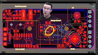
In this particular video, We'll discuss how to use route track tool of KiCad and try to route all the footprints. Also, try to understand basics design principle of routing using some example. Then will discuss how to switch layer using top and bottom copper layer along with via and pads. Finally the video ends with copper filling and verifying the PCB in the 3d viewer.
KiCad Project file : https://github.com/pcbcupid/Kicad-7-Series/tree/main/10_PCB_Routing
You can directly support us on Pateron : https://www.patreon.com/pcbcupid
Like to learn what is PCB? You can check out our website PCB CUPID:
https://pcbcupid.com/
Design rules : https://pcbcupid.com/posts/top-7-pcb-design-guidelines-professional-dont-share/
If you have any question or doubts regarding this video, You can drop your questions here : https://pcbcupid.com/questions/
Make sure to subscribe and share this content with someone who would love this!
▬▬▬▬▬▬ Follow us on other social media platforms! ▬▬▬▬▬▬
Instagram: https://www.instagram.com/pcbcupid/
LinkedIn: https://www.linkedin.com/company/pcbcupid
Twitter: https://twitter.com/pcbcupid
Pinterest: https://in.pinterest.com/pcbcupid/
Reddit: https://www.reddit.com/user/PCBCupid
▬▬▬▬▬▬ Contents of this video ▬▬▬▬▬▬
0:00 - Intro
0:20 - Verify previous setup
1:30 - Routing
2:20- Basic design rules
2:40- Old Generation PCB
3:15- Track fillet
4:02- Auto Track width
4:36 - Manual Track width
5:10 - Routing on bottom layer
5:52 - Via
7:38 - Copper fills
9:06 - outro
#pcb #learning #learn #printedcircuitboard #kicad #electronic #cad #routing #pcbdesigning #howto #begineer #electrical #stackup #pcblayout

 11:13
11:13
 5:52:21
 2:01:32
 1:02:50
 37:29
37:29
 7:58
7:58
 8:33
8:33
 12:16
12:16
 12:52
12:52
 44:57
44:57
 10:40
10:40
 2:25:30
 10:56
10:56
 13:16
13:16
 5:50
5:50
 38:55
38:55
 9:35
9:35
 11:13
11:13
 52:16
52:16