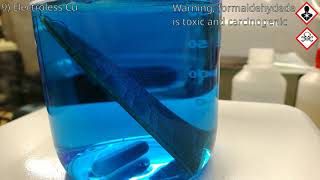
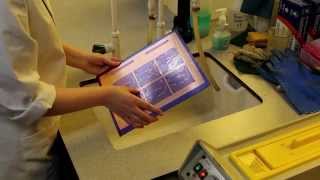
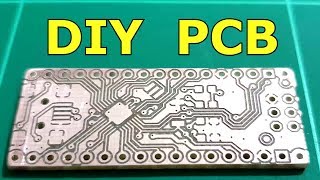
This video presents Process 01, an open source 2 layer PCB production process, including electroless copper plating of vias.
In this first part I will go through all the 31 steps required to make a double sided printed circuit board, while in the next video I will detail the preparation of all chemical solutions required by the process.
https://hackaday.io/project/180422-process-01-an-open-source-2-layer-pcb-process
Other works cited in this video:
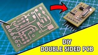
Example of 2 layer PCB without plated vias, using rivets:
https://www.instructables.com/DIY-Professional-Double-Sided-PCB/
Conductive graphite and electroplating process experiments:
https://blog.honzamrazek.cz/2017/10/diy-through-hole-plating-of-pcbs/
Electroless copper plating experiments:
DIY HOMEMADE:
https://www.youtube.com/watch?v=90VN_80zxAQ
guser210:
https://www.youtube.com/watch?v=EEmW4xBFiac
Images used in this video:
Image of PCB factory in the video taken form Wikipedia (https://en.wikipedia.org/wiki/File:PCBs_hanging_in_electroplating_machine.jpg)
1967 PCB photo taken from Wikipedia (https://en.wikipedia.org/wiki/File:S111FlipChipBack.jpg)
1943 PCB photo taken from Wikipedia (https://en.wikipedia.org/wiki/File:Mark-53-proximity-fuze-1943.jpg)
 8:39
8:39
 1:19:29
 27:49
27:49
 6:41
6:41
 32:17
32:17
 26:53
26:53
 14:31
14:31
 44:57
44:57
 8:23
8:23
 12:56
12:56
 5:28
5:28
 1:46:46
 8:59
8:59
 17:10
17:10
 10:56
10:56
 38:17
38:17
 23:34
23:34
 17:32
17:32
 47:57
47:57
 30:48
30:48