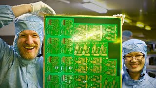
Walking through one of the top PCB factories in China. Recorded in PCBWay: https://www.pcbway.com/
Learn how to design PCB:
- FEDEVEL online courses: https://www.fedevel.com/courses
Chapters:
00:00 What is this video about
00:16 Preparing panel
01:46 Drilling
03:01 Electroless plating
04:31 Cleaning
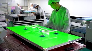
06:04 Photosensitive layer
08:54 Electroplating
10:29 Etching
12:36 Solder mask
14:21 Silkscreen
15:08 PCB Testing
16:06 Milling
16:37 Inspection and packaging
17:39 Making a multilayer PCB
20:04 Baking PCBs
22:23 X-Ray and alignment
23:28 SMT Board assembly
26:30 Through hole soldering
28:45 Thank you for watching
------------------------------------------------------
Would you like to support me? It's simple:
- Sign up for online courses hosted on our platform: https://fedevel.com/
- You can also support me through Patreon: https://www.patreon.com/robertferanec
- FEDEVEL Discord: https://discord.gg/8a8dUcHmrx
It is much appreciated. Thank you,
- Robert

 22:33
22:33
 1:00:01
 25:34
25:34
 1:13:48
 18:37
18:37
 24:57
24:57
 28:30
28:30
 26:49
26:49
 30:42
30:42
 19:56
19:56
 17:18
17:18
 25:39
25:39
 1:19:43
 28:12
28:12
 25:51
25:51
 27:48
27:48
 22:09
22:09
 18:03
18:03
 1:26:05
 8:11
8:11